Chiplet Architecture Revolution: The Future of Semiconductor Design
As Moore’s Law slows and fabrication costs skyrocket, the semiconductor industry is undergoing a fundamental shift. In 2026, chiplet architecture has emerged as one of the most important innovations, enabling manufacturers to build high-performance systems by combining smaller, modular dies instead of a single monolithic chip.
This transition is not just technical—it is economic, strategic, and reshaping the global semiconductor supply chain.
1. What is Chiplet Architecture?
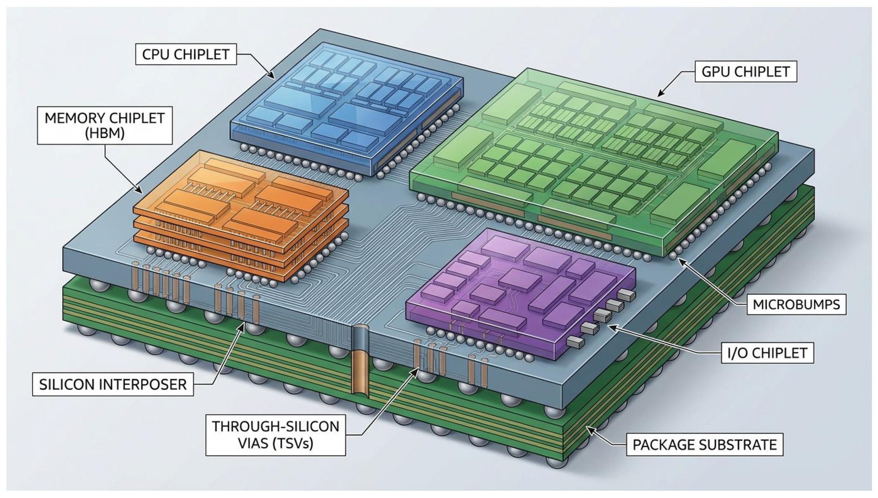
Chiplet architecture involves splitting a complex integrated circuit into smaller functional blocks (chiplets), which are then interconnected within a single package.
- CPU cores
- Memory modules
- I/O controllers
- AI accelerators
These chiplets can be manufactured separately and combined using advanced packaging technologies.
2. Why the Industry is Moving to Chiplets
| Challenge | Monolithic Chips | Chiplet Approach |
|---|---|---|
| Cost | Very high at advanced nodes | Lower due to modular production |
| Yield | Lower for large dies | Higher with smaller dies |
| Scalability | Limited | Highly scalable |
| Time-to-market | Long | Faster iteration |
Chiplets significantly reduce manufacturing risk and improve overall efficiency.
3. Market Growth & Adoption
| Year | Chiplet Market Size | Growth Rate |
|---|---|---|
| 2024 | $7B | - |
| 2025 | $11–13B | ~60% |
| 2030 (forecast) | $80B+ | Explosive growth |
Adoption is accelerating across AI, HPC, automotive, and data center markets.
4. Key Industry Players
| Company | Role | Chiplet Strategy |
|---|---|---|
| AMD | CPU leader | Pioneered chiplet CPUs |
| Intel | Foundry & CPU | Advanced packaging (Foveros) |
| TSMC | Foundry | CoWoS / SoIC packaging |
| NVIDIA | AI leader | Multi-die GPU architectures |
5. Advanced Packaging Technologies
Chiplet success depends heavily on packaging innovations:
- 2.5D Packaging: Interposer-based integration
- 3D Stacking: Vertical die stacking
- Hybrid Bonding: High-speed interconnects
| Technology | Use Case | Advantage |
|---|---|---|
| CoWoS | AI GPUs | High bandwidth |
| Foveros | CPUs | 3D stacking |
| SoIC | Advanced logic | Low latency |
6. Commercial Impact
- Lower production costs for high-performance chips
- Faster innovation cycles
- Improved supply chain flexibility
- Customization for specific industries
This enables companies to build tailored solutions for AI, automotive, and industrial applications.
7. Challenges
| Challenge | Impact |
|---|---|
| Interconnect complexity | Performance bottlenecks |
| Thermal management | Heat dissipation issues |
| Standardization | Lack of universal protocols |
8. Future Outlook
By 2030, chiplet architecture is expected to become the dominant design approach for advanced semiconductor systems.
- AI chips will rely heavily on modular design
- Automotive systems will adopt chiplets for flexibility
- Open standards (like UCIe) will accelerate adoption
Conclusion
Chiplet architecture is not just an innovation—it is a necessity in the post-Moore’s Law era. By enabling cost efficiency, scalability, and faster development, chiplets are reshaping the semiconductor industry.
At Simplytronix, we track these emerging technologies to help businesses stay ahead in an increasingly complex electronics landscape.